


Copper-Plated PCB Boards: Benefits, Properties, and Common Applications
- Harshit Shah

- May 25
- 7 min read
Updated: Jun 2

For OEMs , PCB selection affects more than board performance. It also influences product reliability, production stability, and long-term cost control.
As electronic products handle more power and tighter thermal demands, standard boards may not always deliver the required results in demanding applications.
This is where a copper-plated PCB offers a practical advantage. With better current handling and improved heat dissipation, a copper-plated PCB board can support more reliable products and smoother manufacturing outcomes.
For companies focused on quality, consistency, and performance, understanding the value of copper-plated boards can support better production decisions.
Key Takeaways
A copper-plated PCB improves conductivity, heat dissipation, and overall product reliability.
These boards are widely used in high-power applications such as automotive, industrial, and energy systems.
Copper-plated PCB benefits include improved thermal management, higher current capacity, and greater durability.
However, copper-plated PCB drawbacks include higher cost and more complex manufacturing.
Proper copper-plated PCB design and material selection are important for performance and manufacturability.
Choosing the right PCB assembly manufacturer helps ensure consistent quality and production efficiency.
Table of Contents
What Are Copper-Plated PCB Boards?
A copper-plated printed circuit board includes additional copper plating to improve conductivity and thermal performance. This extra copper helps the board carry higher current and manage heat more effectively.
The copper-plated PCB thickness can vary based on application needs. Boards designed for high-power systems typically use thicker copper, while others balance performance with compact design. The copper-plated PCB material also plays a role in determining strength and reliability.
Key Properties of Copper-Plated PCB Boards
The performance of a copper-plated PCB depends on a few key characteristics:
High electrical conductivity
Efficient heat dissipation
Strong mechanical structure
Ability to handle high current loads
These copper-plated PCB properties make them suitable for demanding electronic systems.
What are the Benefits of Copper-Plated PCB Boards
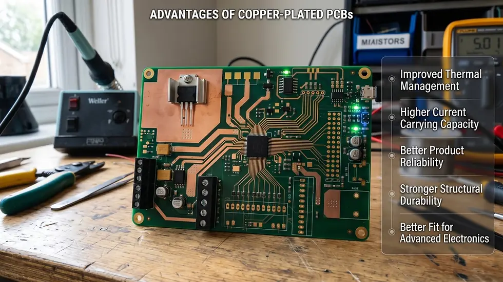
There are many copper-plated PCB benefits, especially in products where performance and durability matter.
Improved Thermal Management
Heat is one of the biggest challenges in electronics. When heat is not controlled properly, it can shorten component life and reduce system stability. A copper-plated PCB helps move heat more efficiently, which supports better product performance over time.
Higher Current Carrying Capacity
Boards with added copper are better suited for circuits that handle heavier electrical loads. This makes them useful in motor controls, power supplies, and battery-related systems.
Better Product Reliability
A board that runs cooler and handles current more effectively is often more dependable in long-term use. This is one of the most practical copper-plated PCB benefits for manufacturers building products for industrial or mission-focused applications.
Stronger Structural Durability
In tough environments, stronger boards matter. Extra copper can improve board stability and reduce the risk of damage from thermal expansion or mechanical stress.
Better Fit for Advanced Electronics
As devices continue to become more compact and more powerful, designers often need PCB assembly solutions that can support higher performance without sacrificing stability. Copper-plated boards help meet that need.
What are the Drawbacks of Copper-Plated PCB Boards
While the advantages are clear, there are also some copper-plated PCB drawbacks to keep in mind.
Higher Production Cost
A copper-plated PCB usually costs more than a standard board because it requires more material and added process control during manufacturing.
More Complex Manufacturing
The copper-plated PCB manufacturing process can be more demanding. Thicker copper affects etching, plating uniformity, and trace definition, so tighter process control is often needed.
Increased Board Weight
Extra copper adds weight. In some applications, this may not matter, but in lightweight products, it can become a design concern.
Design Limitations in Fine-Pitch Layouts
One of the common copper-plated PCB challenges is balancing heavy copper requirements with fine traces and compact layouts. The more copper involved, the more carefully the board must be designed.
What are the Types of Copper-Plated PCB Boards

Common copper-plated PCB types include:
Single-sided PCB – A single-sided PCB has one layer of copper on one side of the board, with all PCB components and traces placed on that same side.
Double-sided PCB – A double-sided PCB has copper layers on both sides of the board, allowing traces to cross and interconnect using plated through-holes or vias.
Multilayer PCB – A multilayer PCB stacks three or more copper layers separated by insulating material, enabling high-density routing for complex and compact electronic designs.
Heavy copper PCB – A heavy copper PCB uses significantly thicker copper (typically ≥3 oz/ft²) to handle higher currents, improved heat dissipation, and robust mechanical strength for power and high-reliability applications.
Each type is selected based on circuit complexity and performance requirements.
You May Also Read: Rigid PCB: Meaning, Types, and Common Applications
Structure of a Copper-Plated PCB Board
A typical copper-plated PCB board includes:
Base substrate (such as FR4)
Copper layers for conduction
Additional plated copper for performance
Protective solder mask
The structure is designed to balance electrical performance and durability.
Read our comparison blog on: FR4 vs. Rogers: Which PCB Material Is Right for Your Project?
What are the Applications of Copper-Plated PCB Boards
The range of copper-plated printed circuit board applications continues to grow:
Power electronics and converters
Industrial equipment
Renewable energy systems
Telecommunications
These applications rely on better heat control and current handling.

Copper PCB Design Considerations and Challenges
Designing a copper-plated PCB requires careful planning. Important PCB design consideration points include:
Selecting the right copper-plated PCB thickness
Managing heat distribution
Designing proper trace width and spacing
Choosing suitable PCB materials
Common copper PCB design challenges include balancing thermal performance with compact layouts and maintaining signal integrity.
You may also read: Why Electronic Contract Manufacturing Services Are Crucial For Modern Electronics Design
Manufacturing and Assembling Process of Copper-Plated PCB Boards
Understanding copper PCB manufacturing and assembly process is key to producing reliable copper-plated PCBs. Manufacturing builds the bare board through copper plating, etching, and drilling, while assembly mounts electronic components onto it. Together, these stages ensure a fully functional, high-performance printed circuit board.
Manufacturing process
The manufacturing process of copper-plated PCB boards begins with preparing a copper-clad laminate, applying photoresist, imaging the circuit pattern, and etching away unwanted copper to form the required traces and pads, followed by drilling vias and through-holes and plating them with copper to create reliable interconnections across layers. After this, the boards receive solder mask, silkscreen, and a suitable surface finish (such as HASL or ENIG), and are electrically tested and inspected to verify continuity and insulation before assembly.
Assembly Process
In the printed circuit board assembly process , SMT and through-hole components are accurately placed on the circuit board, soldered using reflow and wave or selective soldering processes, and then subjected to automated optical inspection, X-ray (for hidden joints like BGAs), and in-circuit or functional testing to ensure the copper-plated circuit board assembly meets performance, reliability, and quality requirements.
How Much Do Copper-Plated PCBs Cost?
The cost depends on:
Board size and complexity
Copper thickness
Number of PCB layers
Production volume
In general, a copper-plated PCB can cost roughly $10 to $100+ per board for low-volume production, depending on specifications. For higher volumes, the copper-plated PCB cost per unit typically decreases due to economies of scale.
Compared to standard PCBs, copper-plated boards are more expensive, but the improved performance and durability often justify the investment, especially in high-power or demanding applications.
You May Also Read: How Much Does PCB Assembly Price?
Future Trends of Copper-Plated PCBs
The demand for copper-plated PCBs continues to grow with:
Expansion of electric vehicles
Growth in renewable energy systems
Increasing need for efficient thermal management
Rising adoption in high-power electronics and energy storage systems
Growth in industrial automation and smart manufacturing
Increased use in advanced telecommunications infrastructure
Demand for compact, high-performance electronic devices
Development of improved copper-plated PCB materials for better durability
Integration with next-generation power management systems
These trends highlight the importance of copper-based PCB solutions in modern electronics.
Read our latest blog on: Top 13 PCB Assembly Trends OEMs Need to Know in 2026
How to Choose the Right Copper-Plated PCB Assembly Manufacturer?
Choosing the right PCB assembly manufacturer is important for product reliability.
Look for:
Experience in copper-plated PCB assembly manufacturing
Strong quality control processes
Ability to handle custom designs
Clear communication and support
A reliable partner helps maintain consistent production quality.
Conclusion
A copper-plated PCB offers better conductivity, improved heat dissipation, and stronger durability compared to standard boards. These features make it suitable for high-performance applications.
While there are some copper-plated PCB drawbacks, the benefits often outweigh the limitations in demanding environments. By understanding the copper-plated PCB properties, applications, and design considerations, manufacturers can build more reliable and efficient electronic products.
FAQs
Are copper-plated PCB boards more expensive than aluminum PCBs?
Yes, copper-plated PCB boards are generally more expensive than aluminum PCBs due to higher material costs and a more complex manufacturing process. However, they offer better conductivity and durability, which can provide better long-term value in high-performance applications.
What is the maximum power capacity a copper base PCB can handle?
The power capacity of a copper-plated PCB depends on factors like copper-plated PCB thickness, trace width, and thermal design. These boards are built to handle higher current loads than standard PCBs, making them suitable for power-intensive applications.
Are copper base PCBs RoHS compliant?
Yes, most copper-plated PCB boards can be manufactured to meet RoHS compliance standards, as long as approved materials and processes are used during production.
What surface finishes work best for copper-plated PCB boards?
Common surface finishes for a copper-plated PCB include ENIG (Electroless Nickel Immersion Gold), HASL, and OSP. The right choice depends on factors such as solderability, durability, and application requirements.
Is copper plating suitable for flexible PCB engineering?
Copper plating can be used in flexible PCBs, but it requires careful copper-plated PCB design to maintain flexibility and avoid cracking. It is typically used in applications where both flexibility and higher conductivity are needed.


